Pcb Layout Recommendations For Bga Packages
Ball grid array (bga) packages having 0.5mm ball pitch require careful attention to printed circuit board (pcb) design parameters to successfully yield reliable and robust assemblies. It contains the required printed circuit board (pcb) layout guidelines, device pin tables, and package specifications.
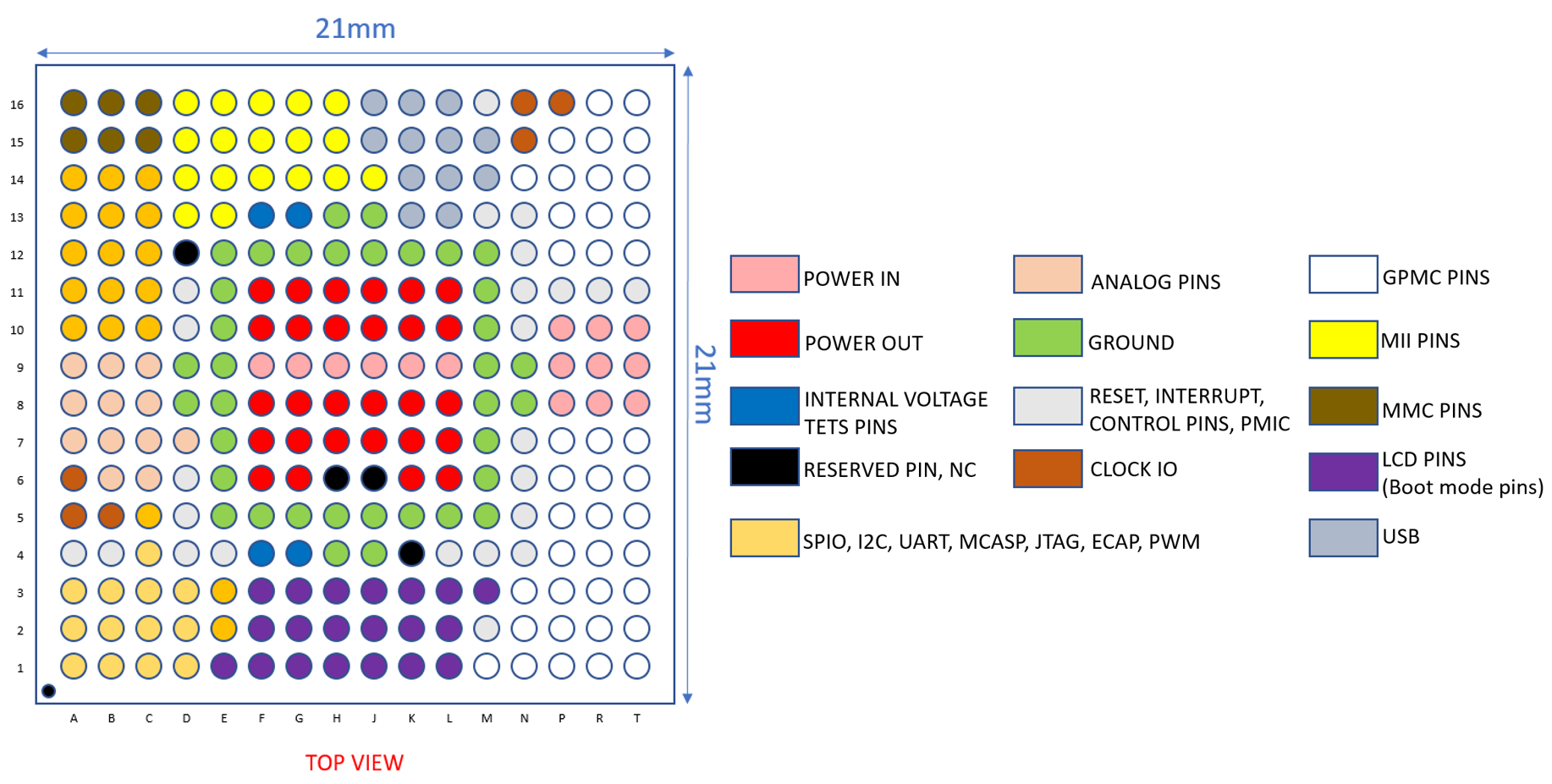
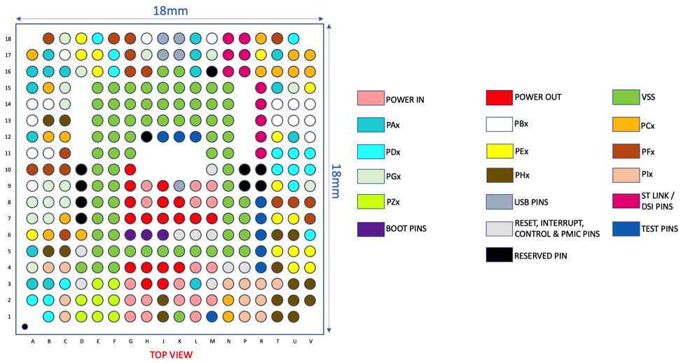
OSD335xSM Layout Guide
Below are some tips to avoid bga design mistakes.

Pcb layout recommendations for bga packages. Learn to leverage the power of your pcb design tools for working with bgas. Solder mask opening should be bga ball size + 0.1mm. Bga packages for embedded design has evolved significantly over the years, to keep up with the technological progression of chip manufacturers.
After soldering, the package looks as if it is pasted on the board with glue. 2 — 15 april 2011 8 of 14. Below are some tips to avoid bga design mistakes.
Regardless of the bga packaging size you must consider what size of pads are required and how many connections are needed to be brought out of the package. The standard rules of thumb don't apply anymore. We have been asked by designers to provide guidelines for bga components on a pcb.
For nsmd pcb land pad dimensions are recommended to be equal to the bga ball size. According to the arrangement mode of solder ball welding, it can be divided into peripheral type, staggered type and full array type bga. Pcb layout guidelines for nxp mcus in bga packages.
The 3d layout of a bga footprint with internal trace routing beneath it. Document revision history for an 114: Bga device design rules www.xilinx.com 6 ug1099 (v1.0) march 1, 2016 chapter 1:
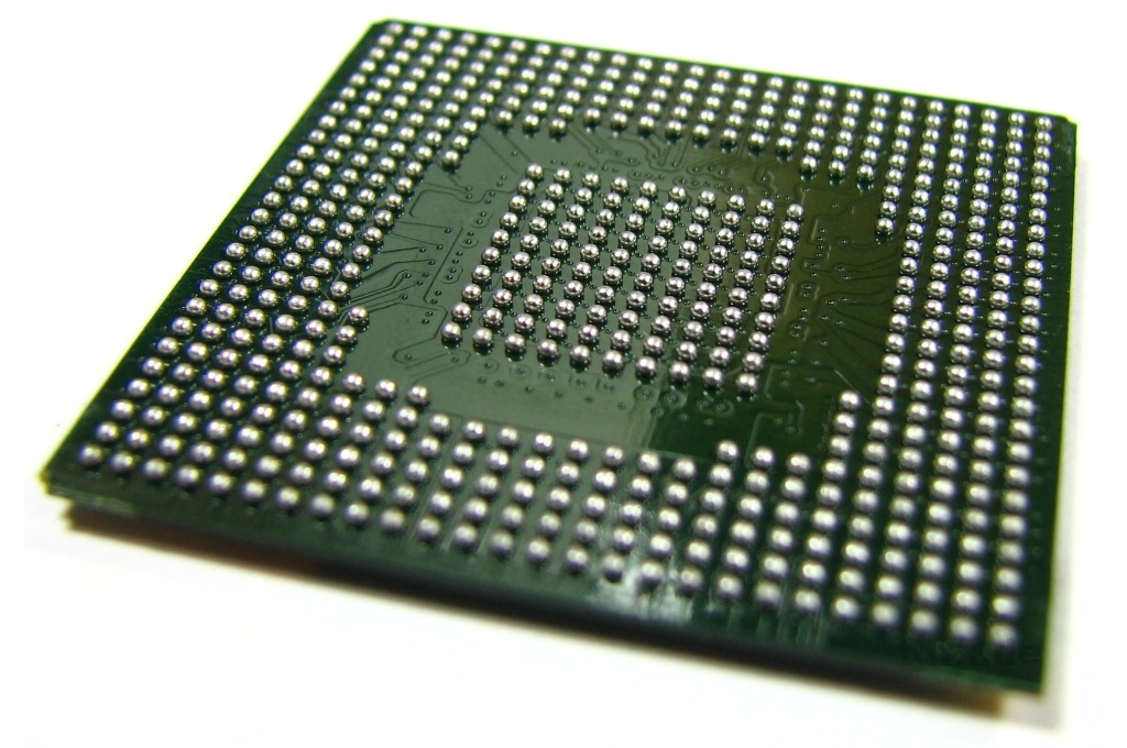
Top 5 effective tips of bga pcb layout guidelines for pcb manufacturing. According to the different substrates, it will divided into. It contains similar connections, just like the ball grid array present on the back of the bga package.
It is recommended that these guidelines be followed to ensure proper thermal and electrical connections. Pcb layout guidelines this section provides information for board layout designers to successfully layout their boards for max® ii devices. Keep in mind that ball size of 0.4mm pitch bgas are smaller than those of 0.5mm pitch bgas.
A layout example incorporating the guidelines in this article is shown in figure 3. Explore pcb layout recommendations for bga packages. Ball grid array (bga) packages having 0.4mm ball pitch require careful attention to printed circuit board (pcb) design parameters to successfully yield reliable and robust assemblies;
The component is placed over the pcb and then soldered. With today's electronics technology, the demand for i/o availability poses a number of challenges, even for. In fact, the design guidelines for 0.4mm and 0.5mm differ primarily due to issues
Examine bga packages in greater detail. The ipc land pattern calculator can be downloaded from the ipc website (www.ipc.org). There are many types of bga packaging;
Keep in mind that ball size of 0.4mm pitch bgas are smaller than those of 0.5mm pitch bgas. For the 0.4 mm land pitch use the via in pad. In order to evenly balance the stress in the solder joints, lattice recommends pcb solder pads be smd with dimensions as similar to the applicable bga as.
The general shape structure is square or rectangular. Definition of pitch size pp pp pp pp pp pp; This section includes the following chapters:
Bga consists of many overlapping layers that include one to a million. The small pitch between bga balls and their matrix arrangement makes it impractical to route all of the bga balls away from the bga on a single layer. Board design guidelines for intel® programmable device packages
As electronic devices continue to grow in their capabilities, they are also shrinking in size at the same time. The pcb used for placing the bga components is known as bga pcb. Overview of bga packages 1.2.
The high di/dt loops on the primary and secondary sides are minimized as. This particular type of packaging can be broken down into standard bgas and micro bgas. Bga is nothing but ball grid array which is a type of surface mount technology ( smt ), and it means soldering between components and pcb.
The via in pad should be micro via, Bga packages are used to permanently mount devices such as microprocessors.
PCB Layout For Bga Packages Printed


Pcb Layout for Bga Packages [PDF Document]
PCB Layout for QFN Packages

PCB LAYOUT AUTHORITY PCB Layout for BGA

Bga Layout Guidelines PCB Circuits

(PDF) Evaluation of PCB layout guidelines for controlling
Ball Grid Array Multi Circuit Boards
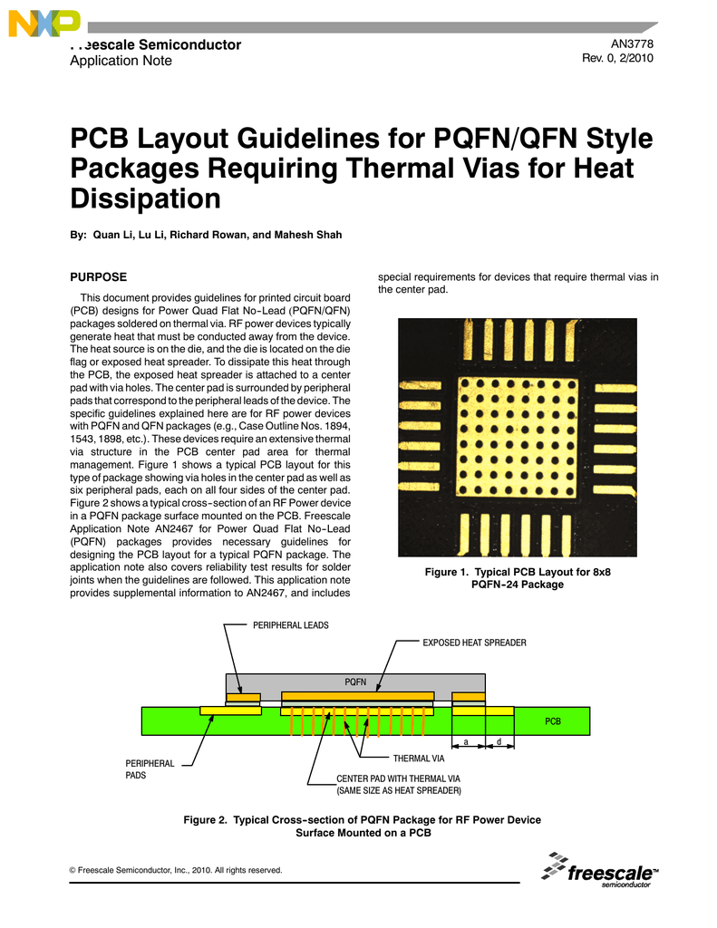
PCB Layout Guidelines for PQFN/QFN Style Packages Requiring
OSD32MP15x Layout Guide STM32MP1 System in Package
PCB Design Guidelines for 0.4mm PackageOn

BGA144C80P12X12_1000X1000X140 PCB 3D

Pcb Layout for Bga Packages [PDF Document]
Bga Layout Guidelines PCB Circuits
How to Successfully Design a BGA PCB Design Blog
Bga Layout Guidelines PCB Circuits

Bga Layout Guidelines PCB Circuits
Pcb Layout for Bga Packages Printed


Pcb Layout for Bga Packages [PDF Document]
PCB Layout for BGA Printed Circuit Board
